We use cookies for optimal website use. We recommend you to allow cookies for a better user experience. Please read our privacy policy. Learn more.
My Account
Search

Features
- Operating voltage: 3.0V – 5.5V
- Operating current:
0.5uA(Typ.) @ 5V, deep sleep mode
3.2mA(Typ.) @ 5V, receiving mode - RX sensitivity: -112dBm(Typ.)@ 5V, 25℃, 10Ksps
- Maximum operating input power: 10dBm@RF-in, BER=0.1%
- Modulation: OOK
- Symbol rate: 1Ksps – 20Ksps
- Operating Temperature: -40℃- 85℃
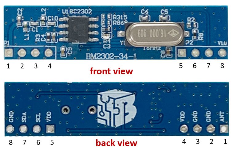
Pin Function
- Pin 1: ANT, connect to 50 ohm impedance antenna
- Pin 2,3,8: GND, ground
- Pin 4,5: VDD, power supply,3.0V – 5.5V.
- Pin 6: SD/SCL,
SD: RX mode shut-down control, it should be pulled low in RX Mode.
SCL: I2C clock input line in Configuration Mode. - Pin 7: DO/SDA,
DO: demodulated data output in RX Mode
SDA: I2C data line in Configuration Mode
Operation Mode
After powered on, this module is in deep sleep mode, in which it consumes 0.5uA only. With the proper control of the DO/SDA and SD/SCL pins, this module can work in configuration mode or receiving mode (RX mode).
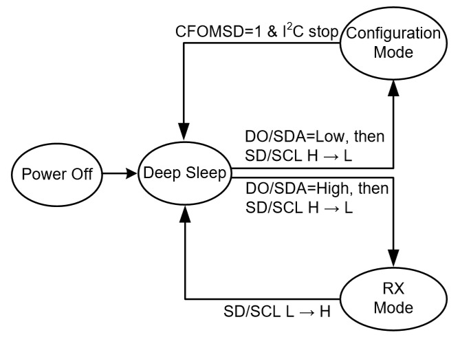
1. Auto RX mode
Wire connection: Connect the SD/SCL pin to ground (GND).
After powered on, the module works in Auto RX mode automatically. The module will continuously receive the RF signal from the antenna and output the demodulated data to the DO/SDA pin. The module will remain in this mode until the power is removed.
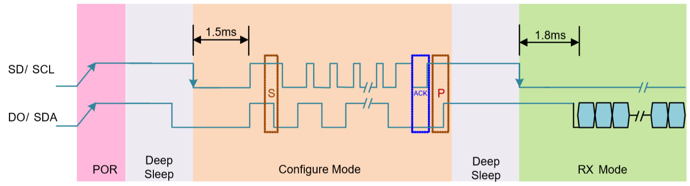
The below image is the output waveform with the BCR-68F2130-X01 as the transmitter. You may need an MCU to decode the waveform. Refer to the AN0515 BC2302A/B Development Board Application Note for example program.

2. Sniff RX mode
Wire connection: Connect the SD/SCL pin to an MCU.
After powered on, the module is in deep sleep mode. Both the SD/SCL and DO/SDA pins are in high level due to the internal pull-up resistors of the BC2032. The external MCU can control the SD/SCL pin to switch the operation mode, low for the receiving mode, high for the deep sleep mode.
3. Configuration mode
Wire connection: Connect both the SD/SCL and DO/SDA pins to an MCU.
After powered on, the external MCU uses the I2C interface to configure the BC2302 chip. Refer to the BC2302 datasheet for details. Normally it is not necessary to configure this module unless you want to do advance settings.
Product Information
- Dimension: 43.0 x 10.5 x 5.2(mm)
- Weight: 1.7g
- Packing List:
- BM2302-34-1 module x 1
Resources
IC: Holtek BC2302A/BC2302B, Sub-1GHz Low-IF OOK RF Receiver| HS Code (reference) | 8517.79.00.00-6 |
|---|
Related Products